

Semiconductor Plating

About Semiconductors Plating
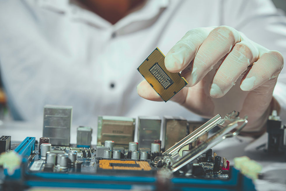
Semiconductor Plating Services
Titan Plating provides specialised plating services for semiconductors, the cornerstone of modern electronics, powering devices from smartphones and laptops to automotive systems and industrial robotics. Our precision coatings protect semiconductor components, such as transistors and chips, while enhancing their connectivity and performance in demanding applications.
Importance of Semiconductor Plating
Semiconductors, typically made from silicon, rely on plating to shield their delicate structures from environmental damage and to facilitate electrical connections. The outer metal coating acts as a protective barrier and an interactive layer, ensuring reliable signal transmission and durability. Titan Plating’s tailored solutions meet the rigorous demands of the electronics industry, supporting high-quality production across various sectors.
Semiconductor production involves several stages, with plating as a critical final step:
-
Wafer Production: Purified semiconductor material, usually silicon, is heated, moulded, and processed into thin, smooth wafers.
-
Deposition: Wafers are cleaned, heated, and exposed to oxygen in a diffusion furnace, forming a uniform silicon dioxide film.
-
Masking (Photolithography): A light-sensitive film is applied, and intense light projects a mask pattern onto the wafer, defining areas for further processing.
-
Etching: The wafer is baked to harden the film pattern, then exposed to a chemical solution to remove unprotected areas, ensuring accurate pattern transfer.
-
Doping: Boron or phosphorus atoms are introduced to alter electrical properties, creating N-type (negative) or P-type (positive) regions for conductivity.
-
Dielectric Deposition and Plating: Metal and insulating layers are added to connect circuits and protect them, with openings etched for external connections.
Plating completes the process, providing a robust interface between the semiconductor’s internal circuits and external systems.
Plating Processes for Semiconductors
Electroplating
Electroplating deposits a thin metal layer onto the semiconductor substrate using an electric current. The substrate (cathode) and plating metal (anode) are immersed in an electrolyte bath, where a DC current oxidises metal atoms, dissolving them into the solution. These atoms then reduce and bond to the substrate, forming a uniform coating. This method is ideal for precise applications requiring conductivity and protection.
Electroless Plating
Electroless plating uses a chemical reaction to deposit metals like nickel, achieving uniform coatings without electricity. This is particularly effective for complex geometries, ensuring consistent coverage on intricate semiconductor surfaces.
Plating Materials for Semiconductors
Selecting the right material optimises semiconductor performance:
-
Tin: Cost-effective, corrosion-resistant, and solderable, tin is ideal for electrical contacts. However, it risks forming whiskers, which can cause shorts, mitigated by using tin-lead alloys or careful process control.
-
Copper: Highly conductive and ductile, copper is used for undercoating or direct plating on contacts and interconnects, though protective layers prevent oxidation.
-
Silver: Offers superior conductivity and solderability, perfect for high-frequency circuits and EMI shielding. Anti-tarnish treatments maintain performance.
-
Gold: Provides excellent conductivity, corrosion resistance, and solderability. Thin gold layers, often over nickel to prevent diffusion, are used for high-reliability applications like connectors and lead frames, despite higher costs.
-
Palladium and Palladium Alloys: Palladium-cobalt and palladium-nickel alloys offer corrosion resistance and low contact resistance. Less dense than gold, they reduce weight and costs, making them a viable alternative for connectors and lead frames.
-
Platinum: Rare and expensive, platinum’s smooth, durable surface protects low-voltage contacts. Its use in fuel cell electrodes highlights its potential for eco-friendly applications.
Benefits of Semiconductor Plating
Our plating services deliver:
-
Enhanced Conductivity: Improves signal transmission and reduces resistance, critical for high-performance electronics.
-
Corrosion Protection: Shields semiconductors from moisture, chemicals, and oxidation, extending lifespan.
-
Improved Solderability: Ensures reliable connections during assembly, minimising failures.
-
Durability: Strengthens components against wear and environmental stresses.
-
Eco-Friendly Options: Palladium and other alternatives reduce reliance on heavy metals like lead, aligning with environmental standards.
Choosing the Right Plating Material
Key considerations include:
-
Appearance: Gold or silver enhances aesthetics for visible components.
-
Damage Prevention: Avoid metals like tin if whisker formation is a concern.
-
Application Requirements: Ensure coatings meet performance specifications, such as conductivity or thermal resistance.
-
Lifespan: Select durable coatings to match or extend product life.
-
Environmental Impact: Prioritise eco-friendly materials to minimise ecological harm.
-
Material Interactions: Use intermediary layers (e.g., nickel under gold) to prevent diffusion and maintain coating integrity.
Titan Plating’s Semiconductor Expertise
Titan Plating offers comprehensive plating solutions, including tin, copper, silver, gold electroplating, and electroless nickel and palladium plating. Our processes ensure precision for applications in consumer electronics, automotive, and industrial sectors. We provide tailored coatings for prototypes and high-volume production, with consulting to optimise material selection for performance and cost. Our efficient processes deliver reliable results, supporting critical semiconductor applications with consistent quality.

Get in touch with Titan Plating
Whether you need expert advice or a custom quote, our team is here to help. Reach out today to discuss your project.